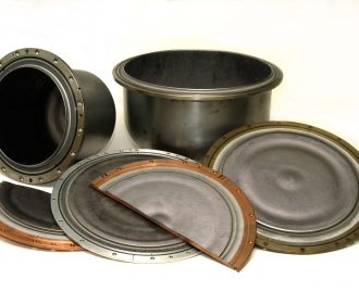
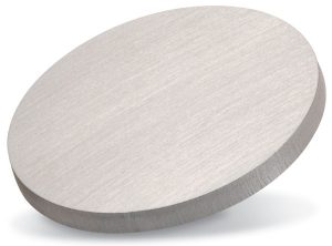
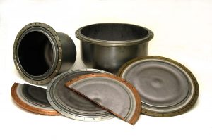
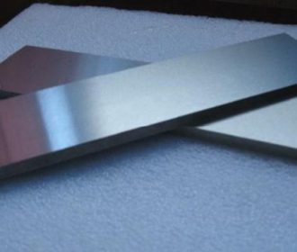
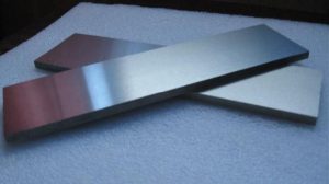
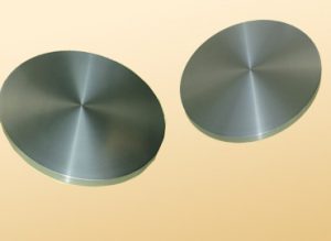
Tantalum sputtering target material is a chip of tantalum obtained by pressure processing. It has high chemical purity, small grain size, as well as good recrystallized structure and consistency of three axes. Tantalum sputtering target is mainly used in optical fiber, the semiconductor chip and integrated circuit sputtering deposition film, as well as in cathode sputtering coating, high vacuum suction active material, etc., which is an important material for thin film technology.
Classification of the tantalum target
According to the application field, it can be divided into optical tantalum target and semiconductor tantalum target.
The performance index of the tantalum target
- Purity
Metal impurities do not affect the sputtering process but affect the life of tantalum film, and the purity of the target material is different in different application fields. The impurities U, Th, and other radioactive elements have a negative impact on MOS, while K, Na and other alkali metals have a negative impact on MOS interface performance. In addition, transition metals such as Fe, Ni, Cr and refractory metals such as W, Mo, and Nb generate leakage current at the interface. Therefore, the content of the above impurity elements should be strictly controlled.
- Porosity
The target material should be dense enough. If there are pores in the target material, the gas in the pores will be released in the sputtering process, and an arc will be generated, causing tiny particles to sputter out of the target and generating uneven points on the film.
- Grain size
The size of grain affects sputtering uniformity and sputtering speed. Typically, the grain size is required to be less than 100 microns, since the large grain size causes uneven sputtering and irregular nodules on the target. Meanwhile, no crystal band is allowed and the grains should be uniform on the whole target surface.
- Texture
The texture difference has a great influence on sputtering speed, and (100) texture is usually required.
- Surface finishingment
If the surface finish of the target material is not high enough, it is easy to form small bumps in the sputtering process.
- Uniformity
Uniformity should be consistent in all directions of the target and between each target.
Applications of the tantalum target
In recent years, with the rapid development of semiconductor technology, electronic devices are becoming more and more miniaturized and integrated, and the thin film technology is used in the manufacturing process.
Tantalum target is mainly used for sputtering coating. Tantalum film, tantalum alloy film, silicon tantalum oxide film, tantalum nitride film, and tantalum oxide film have a wide range of applications. Tantalum oxide is used in the resistance and capacitance of integrated circuits and the resistance of hybrid circuits; tantalum film forms a barrier layer to prevent corrosion when spraying printed circuit; tantalum film is also used as seed in magnetic resonance devices. The total global demand in these areas is about 30t annually.
Another major use of tantalum is as a diffusion barrier between silicon and copper conductors in integrated circuits. Compared with other metals, tantalum, as a barrier layer of copper, has a lower diffusion rate, higher interlayer bonding strength, and heat resistance. The global demand for sputtering targets in this application field is expected to increase to 200t.
Please visit http://www.samaterials.com for more information.
Recent Comments